Please I need design calculation for this circuit And what i
Please I need design calculation for this circuit.
And what is the benefit of each component
D1 R7 4M7 N4001 RELAY RV1 470K D2 1N4001 C1 100n 10uF IC1 04 05 06 07 RTC 08 09 010 012 CTC 013 014 150K RS Q1 BC547 Q4-Q14 R5 4K7 14 4060 R1 100k MR R4 4.7k R6 4.7k LED LED GADGETRONICXSolution
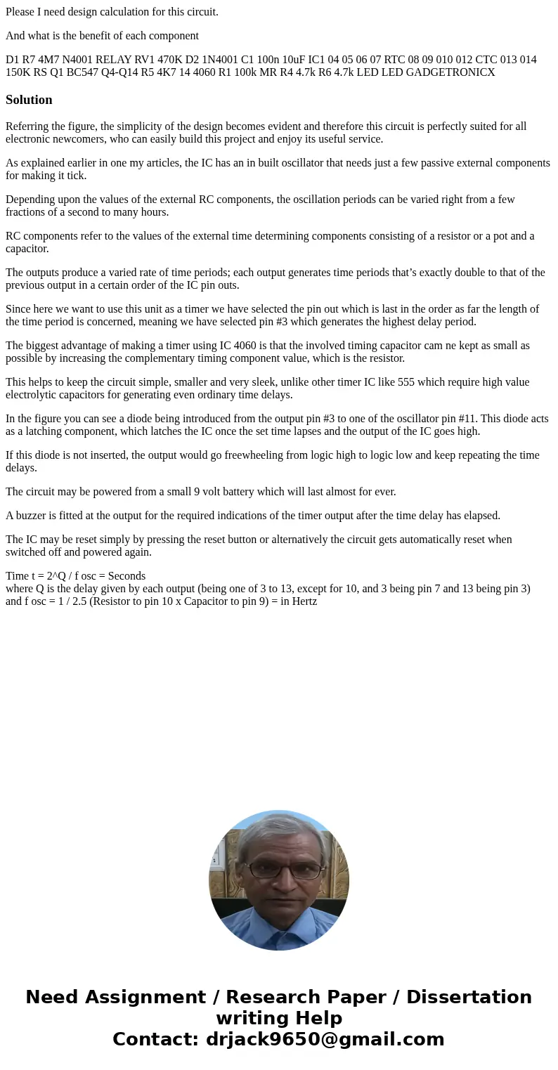
Referring the figure, the simplicity of the design becomes evident and therefore this circuit is perfectly suited for all electronic newcomers, who can easily build this project and enjoy its useful service.
As explained earlier in one my articles, the IC has an in built oscillator that needs just a few passive external components for making it tick.
Depending upon the values of the external RC components, the oscillation periods can be varied right from a few fractions of a second to many hours.
RC components refer to the values of the external time determining components consisting of a resistor or a pot and a capacitor.
The outputs produce a varied rate of time periods; each output generates time periods that’s exactly double to that of the previous output in a certain order of the IC pin outs.
Since here we want to use this unit as a timer we have selected the pin out which is last in the order as far the length of the time period is concerned, meaning we have selected pin #3 which generates the highest delay period.
The biggest advantage of making a timer using IC 4060 is that the involved timing capacitor cam ne kept as small as possible by increasing the complementary timing component value, which is the resistor.
This helps to keep the circuit simple, smaller and very sleek, unlike other timer IC like 555 which require high value electrolytic capacitors for generating even ordinary time delays.
In the figure you can see a diode being introduced from the output pin #3 to one of the oscillator pin #11. This diode acts as a latching component, which latches the IC once the set time lapses and the output of the IC goes high.
If this diode is not inserted, the output would go freewheeling from logic high to logic low and keep repeating the time delays.
The circuit may be powered from a small 9 volt battery which will last almost for ever.
A buzzer is fitted at the output for the required indications of the timer output after the time delay has elapsed.
The IC may be reset simply by pressing the reset button or alternatively the circuit gets automatically reset when switched off and powered again.
Time t = 2^Q / f osc = Seconds
where Q is the delay given by each output (being one of 3 to 13, except for 10, and 3 being pin 7 and 13 being pin 3)
and f osc = 1 / 2.5 (Resistor to pin 10 x Capacitor to pin 9) = in Hertz

 Homework Sourse